Syenta Semiconductor Packaging Technology Company to come to Tempe
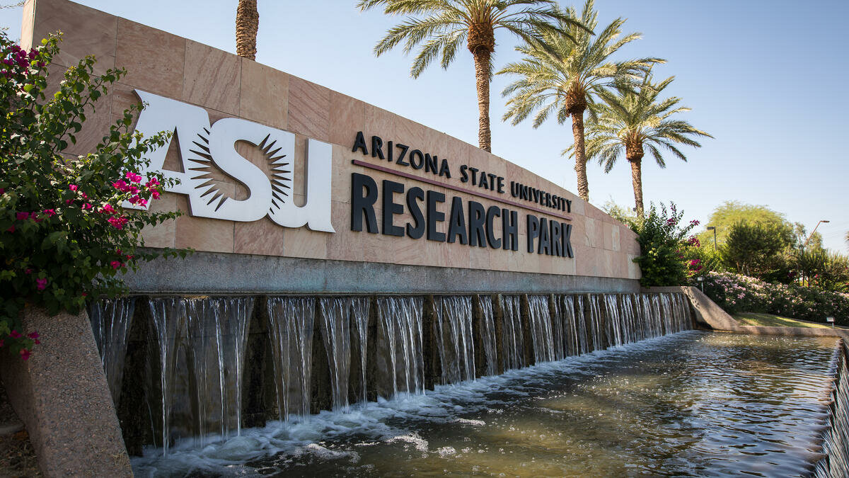
ASU Research Park currently has ground leases with 24 different lessees, in 26 buildings totaling 2.2 million square feet.
Charlie Leight/ASU Now
Syenta, an Australian semiconductor technology company, announced the opening of its first U.S. facility in Tempe, Arizona, bringing advanced packaging technology, high-skilled jobs, and global innovation to the state.
As AI systems push beyond traditional chip design limits, performance is increasingly constrained by advanced packaging, the density and efficiency of chip-to-chip interconnects. Syenta's Localized Electrochemical Manufacturing technology addresses this bottleneck.
The company's new Tempe facility positions it at the center of the U.S. semiconductor industry, where it will extend Syenta’s capability through commercial relationships with customers, research institutions, talent, and partners driving next-generation AI computing.
You must be a member to read this story.
Join our family of readers starting at $5 for your first month and support local, unbiased journalism.
Click here to see your options for becoming a subscriber.
Register to comment
Click here create a free account for posting comments.
Note that free accounts do not include access to premium content on this site.
I am anchor
Technology
Syenta Semiconductor Packaging Technology Company to come to Tempe
Charlie Leight/ASU Now
ASU Research Park currently has ground leases with 24 different lessees, in 26 buildings totaling 2.2 million square feet.
Posted
Syenta, an Australian semiconductor technology company, announced the opening of its first U.S. facility in Tempe, Arizona, bringing advanced packaging technology, high-skilled jobs, and global innovation to the state.
As AI systems push beyond traditional chip design limits, performance is increasingly constrained by advanced packaging, the density and efficiency of chip-to-chip interconnects. Syenta's Localized Electrochemical Manufacturing technology addresses this bottleneck.
The company's new Tempe facility positions it at the center of the U.S. semiconductor industry, where it will extend Syenta’s capability through commercial relationships with customers, research institutions, talent, and partners driving next-generation AI computing.
“Tempe is a natural choice for our first U.S. operations,” said Jekaterina Viktorova, CEO and Founder of Syenta. “The city offers world-class talent, research collaboration, and an ecosystem that allows us to scale our advanced packaging technology in support of AI system performance worldwide. We’re excited to bring our innovation here to be closer to our customers and grow a talented, mission-driven team.”
Tempe officials agree.
"Tempe is where innovators thrive, and we're thrilled to welcome Syenta into our community," said Tempe Mayor Corey Woods. "By choosing our city for its first U.S. facility, Syenta is tapping into one of our region's strongest ecosystems for semiconductor engineering and advanced manufacturing."
Located at ASU Research Park, the new 3,500-square-foot facility will support 200 new highly-skilled roles in semiconductor engineering, systems architecture, and advanced manufacturing, positioning Tempe as a hub for next-generation advanced packaging technologies.
Arizona has become a leading destination for semiconductor development. The city’s robust innovation ecosystem, access to top talent, and research partnerships—including ASU’s Research Park—made Tempe an ideal location for Syenta’s U.S. expansion.
“Syenta’s decision to launch its U.S. operations in Tempe reinforces Arizona’s position as North America’s most advanced and competitive semiconductor ecosystem,” said Sandra Watson, President and CEO of the Arizona Commerce Authority. “This new facility strengthens a critical part of the supply chain and accelerates next‑generation packaging innovation right here in Arizona.”
Global Momentum and Ongoing Growth
While the Arizona expansion is anchored by ACA support, Syenta is also experiencing global growth momentum. Recently, the company announced $26 million in Series A1 funding, led by Playground Global and Australia’s National Reconstruction Fund, to expand advanced packaging capacity and strengthen global supply chains.
Growing the Team
With operations spanning Australia and the United States, Syenta is actively hiring for roles in process and applications engineering.
“We are building a team that is motivated by playing a role in the next frontier of semiconductor manufacturing technology,” said Jekaterina Viktorova. “Every employee contributes directly to the goal of enabling a more efficient chip architecture and manufacturing method for building advanced packaging. We invite talented professionals to join us in Tempe or Sydney.”



Comments
No comments on this item Please log in to comment by clicking here