ASU Research Park chosen for flagship semiconductor facility
Effort is part of CHIPS for America between federal, state and local organizations
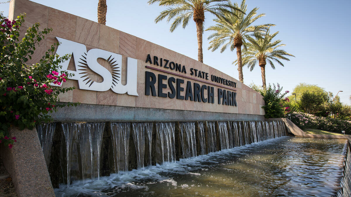
ASU Research Park currently has ground leases with 24 different lessees, in 26 buildings totaling 2.2 million square feet.
Charlie Leight/ASU Now
Arizona State University’s Research Park in Tempe will be the location of a new research and development site involving semiconductor manufacturing.
The U.S. Commerce Department and Natcast, the operator of the National Semiconductor Technology Center, have selected ASU as the site of the co-located NSTC Prototyping and NAPMP Advanced Packaging Piloting Facility.
This marks the third CHIPS for America research and development flagship facility, a city of Tempe release stated. The facility aims to speed up what officials called the “lab-to-fab innovation cycle.”
You must be a member to read this story.
Join our family of readers starting at $5 for your first month and support local, unbiased journalism.
Click here to see your options for becoming a subscriber.
Register to comment
Click here create a free account for posting comments.
Note that free accounts do not include access to premium content on this site.
I am anchor
Research and Development
ASU Research Park chosen for flagship semiconductor facility
Effort is part of CHIPS for America between federal, state and local organizations
Charlie Leight/ASU Now
ASU Research Park currently has ground leases with 24 different lessees, in 26 buildings totaling 2.2 million square feet.
Posted
ASU Research Park 8750 S Science Drive Tempe, AZ 85284
View larger map
Independent Newsmedia
Arizona State University’s Research Park in Tempe will be the location of a new research and development site involving semiconductor manufacturing.
The U.S. Commerce Department and Natcast, the operator of the National Semiconductor Technology Center, have selected ASU as the site of the co-located NSTC Prototyping and NAPMP Advanced Packaging Piloting Facility.
This marks the third CHIPS for America research and development flagship facility, a city of Tempe release stated. The facility aims to speed up what officials called the “lab-to-fab innovation cycle.”
Key packaging capabilities are expected to include an advanced packaging piloting line to enable the development and commercialization of new packaging processes, the release stated. Packaging is a process of taking semiconductors and putting them into forms used by commercial and industrial equipment.
The facility also will support U.S. workforce development efforts by providing opportunities for collaborative, hands-on research using industry-leading tools and equipment.
Tempe Mayor Corey Woods said in the release the city thanks its partners at the Arizona Commerce Authority and ASU for developing a “world-class” research ecosystem to serve the community and beyond.
“Tempe and Arizona continue to be at the center of groundbreaking research and development, leading the way in next-generation technology,” Woods said. “We are proud to be the home of this new flagship facility that will serve as a hub for semiconductor innovation nationwide.”
The facility, at 8240 S. River Parkway, represents a partnership and co-investment among the Department of Commerce, Natcast, the state of Arizona, Arizona Commerce Authority and ASU.
It is expected to be operational as early as fourth-quarter 2028, the release stated.
As part of its engagement in this project, ASU will provide immediate access to ASU Core Research Facilities; Natcast and NAPMP researchers as well as NSTC members will have access to ASU’s cutting-edge resources, including the MacroTechnology Works.
The Arizona State University Research Park celebrated its 40th anniversary this year. This dynamic space houses leading tech companies such as Viasat, Amkor Technologies and Applied Materials.
Officials said they believe the partnership with ASU will jump-start research and development in these areas and leverage the programs underway at the university, solidifying Arizona’s place at the center of America’s advanced manufacturing economy and opening pathways for continued business investment and job growth.
U.S. Secretary of Commerce Gina Raimondo said in the release that a strong research and development ecosystem is essential to keeping the country at the forefront of semiconductor innovation.
“Arizona has long been a hub for technological progress, and this new facility will strengthen our domestic supply chain, drive advanced manufacturing breakthroughs, and secure America’s leadership in this critical industry,” Raimondo said.
Sandra Watson, president and CEO of the Arizona Commerce Authority, said in the release this announcement shows how robust Arizona’s semiconductor ecosystem is, along with the national network of industry and research partners advancing technology innovation.
Elected leaders from around the state also recognized the significance of this new facility. Gov. Katie Hobbs said in the release this announcement solidifies Arizona’s position as a global hub for advanced manufacturing and innovation.
“This flagship facility will serve as an anchor for Arizona’s thriving semiconductor ecosystem while supporting R&D and supply chain resiliency nationwide,” Hobbs said.
Other leaders who shared their excitement for this local announcement in the release included Sen. Mark Kelly, Sen. Ruben Gallego and Rep. Greg Stanton.
“Thanks to our CHIPS Act, this new Advanced Packaging Piloting Facility at ASU will help develop the next-generation technology America needs to compete and win on the world stage–and train the future of the semiconductor workforce here at home,” Stanton said.
For information about opportunities in Tempe, visit tempe.gov/EconomicDevelopment.



Comments
No comments on this item Please log in to comment by clicking here